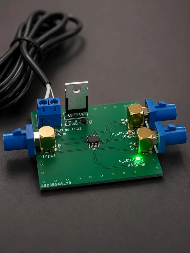
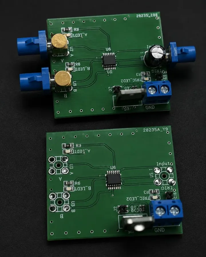
RF Band-Pass Filter
Passive microstrip RF filter board designed to attenuate out-of-band signals while passing a selected frequency band.
Project overview
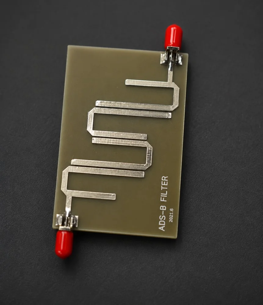
Passive microstrip RF filter board designed to attenuate out-of-band signals while passing a selected frequency band.
Engineering approach
RF and microwave PCB work depends on controlled impedance and careful trace geometry, since even small layout mistakes at these frequencies show up directly as signal loss. On this board, that translates into a component set built around 2L and Microstrip filter, with layout and stack-up decisions driven by impedance-controlled routing, trace geometry, and minimizing insertion loss across the target frequency range.
Technical specification
Engineering focus
This portfolio project demonstrates CircuitNexa's electronics engineering and PCB design work in the rf pcbs space. The design shown here is part of a broader portfolio spanning schematic capture, PCB layout, embedded firmware, prototyping, and support through to manufacturing.
Building a hardware product?
CircuitNexa helps startups and engineering teams turn electronics concepts into manufacturable hardware.
Talk to CircuitNexa